We would like to present our technique of testing PCBs for reliability, functionality and to assure that they meet our standards – automated bed of nails PCB testing equipment.
What is bed of nails for PCB testing?
PCBs are usually tested with special type of fixture that is made from spring loaded pins to connect to the specially prepared spots (nodes) on the PCB. That type of fixture is named after its appearance. It is a flat surface with pins protruding from it. It allows easy and reliable contact with the PCB and makes it efficient in quickly swapping multiple PCBs for testing.
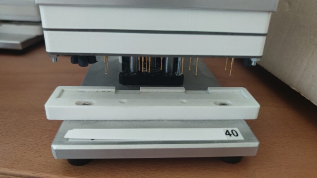
Once the PCB under test is properly aligned with the spring loaded pins on the “bed of nails” it is lowered onto the PCB and pressure is applied so that all the pins are making a good contact with the PCB under test. Cables from the mentioned pins are then routed to the specially designed electronics that measures and test the different functionalities of PCB under test.
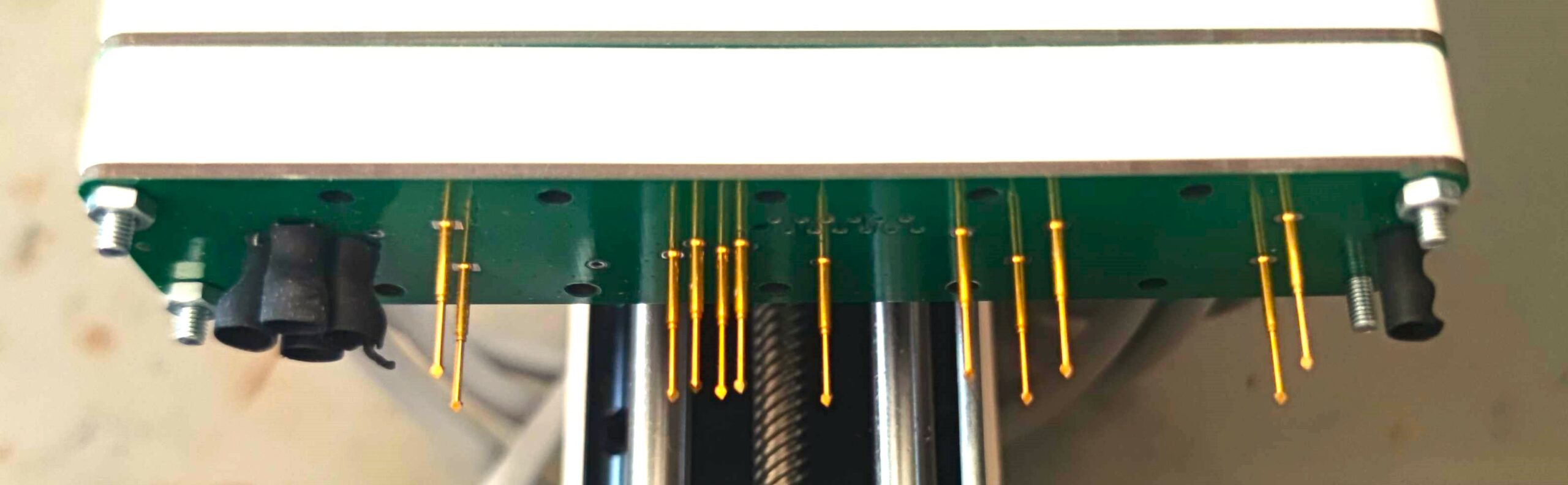
Sprint loaded pins – POGO pins
Spring loaded pins that are used in the bed of nails are also called pogo pins. They are ensuring good and reliable contact with the PCB and have integrated springs to apply pressure and make electrical contact even better.
There are many different types of spring loaded pins, but special consideration has to be taken into account when designing the “bed of nails” test fixture to use the proper type of pogo pins. There are different types of pogo pins available for different test points. If there is simple test point on the PCB the pointed pin is usually used, but for connection to the already soldered pin of for instance screw terminal, special pogo pin with “crown” has to be used.
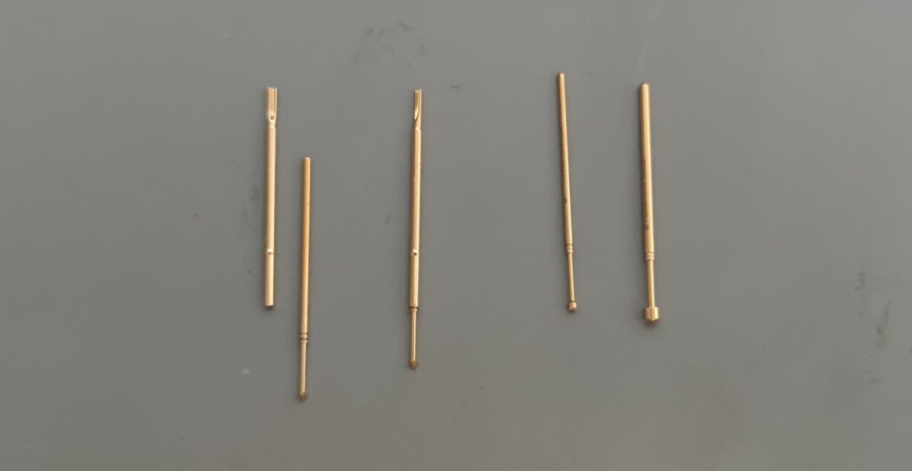
There are also different qualities of pogo pins available. It has to be taken into account, how many test PCBs are intended to be tested. Pogo pins have limited number of cycles and cheaper pogo pins can fail much quicker. There are also pogo pins available that have special sleeve that they are inserted in. That way the pogo pins can be exchanged quickly after intended number of cycles.
Automated motion of bed of nails PCB testing
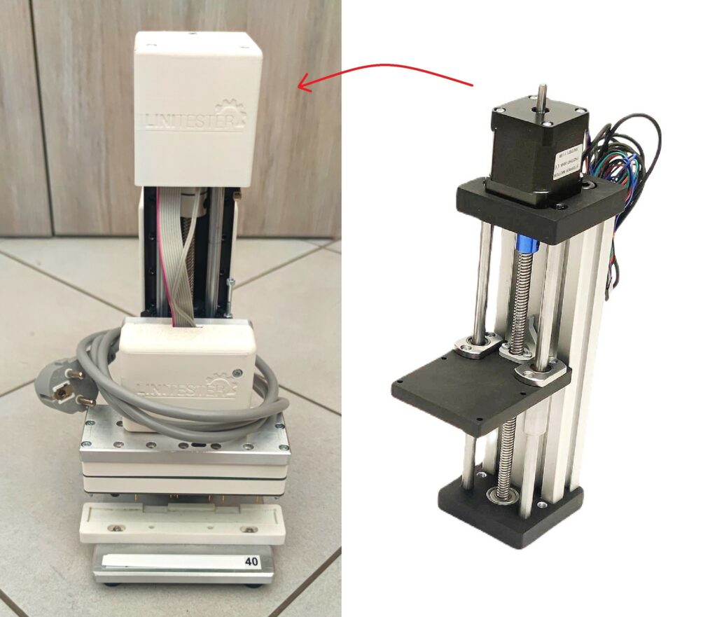
We have developed two different types of automated bed of nails PCB testers for our own use – linitester. There is one for automated testing of PCB panels, where 20 of same PCB under test are mounted on one panel. The testing machine is similar to the CNC machine with Y and Z axis. The test head is mounted on the machine and the test head itself can test 5 PCBs at once. Then it retracts, moves in Y direction and test the next 5 PCBs until all 20 individual PCBs are tested.
The much simpler version of the test machine is single linear axis actuator that moves the bed of nails up and down. The PCB under test is individually manually placed under the test machine which then loweres and pressurizes the pogo pins onto the PCB. The special electronics performs the test on the PCB and then retract the test machine to swap the PCB.
PCB testing limitations
The test head has to be specially designed different PCBs under test. The test points that the pogo pins interface with are usually randomly placed on the PCB so pogo pin locations are different for each different PCB design. PCB is also placed in the receiving part of the automated PCB testing machine which has to be specifically designed for each different PCB design.
For complex PCBs bed of nails PCB testing head can be expensive to design and manufacture. Especially if they have a lot of test points, the number of pogo pins is high as well as all the connections to the electronics. The electronics for testing the PCB under test also has to be custom designed with test procedure in mind. Special features or complex algorithms has to be implemented to properly test the PCB under test.
Wear of the bed of nails PCB testing head also has to be considered. The pogo pins are usually the parts that experience the most wear and tear. If the fixture is designed with that in mind, the pins can be easily replaced in their sleeves with new ones.
Benefits of automated testing
The defects in soldering process are all but uncommon. The impurities, unreliable processes, damaged components etc. all lead to PCBs that are not functional right out of production.
The PCBs that are individually tested show the highest reliability and almost perfect rate of functioning as intended. All the bad PCBs can be taken out of the batch and prevented to be sent to customers. The automated testing is the easiest and most reliable way to ensure good and reliable products.
Related Posts